
News classification
Contact us
- Add: ChanFu Dong Road,XiaoBian Village, ChangAn Town,DongGuan City,GuangDong,China
- Tel: +8613652508770(Jerry )
- Fax: 0769-23094426
- Email: [email protected]
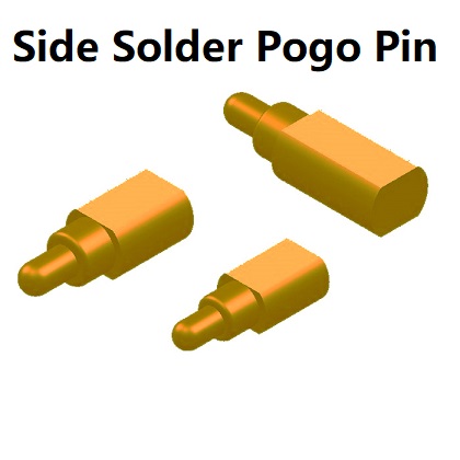
How to Design a Solder Cup Pogo Pin?
How to Design a Solder Cup Pogo Pin?
A Solder Cup Pogo Pin is a type of electrical connector that is frequently used in high-precision applications, such as testing and interconnects in electronic devices. The solder cup design is an essential feature that allows for an easy and secure attachment to a printed circuit board (PCB) by soldering the pin directly onto the board. This design is particularly useful in applications requiring frequent connections, such as automated testing equipment (ATE), medical devices, and consumer electronics.
Designing a solder cup pogo pin requires careful consideration of mechanical, electrical, and material factors to ensure optimal performance and reliability. Below is a detailed guide on how to design a solder cup pogo pin, focusing on key aspects such as material selection, mechanical design, electrical performance, and manufacturing considerations.
1. Understanding Pogo Pin Structure
A typical pogo pin consists of several components:
Pin (Contact) Part : This is the conductive portion of the pogo pin that makes contact with the corresponding contact point on a PCB or another device.
Spring : The spring provides the necessary force to push the contact pin against the target, ensuring a stable electrical connection.
Solder Cup : This is the cup-shaped portion of the pogo pin where the pin is soldered onto a PCB. The solder cup allows for a secure attachment of the pogo pin to the board, which is essential for maintaining long-term reliability and minimizing the risk of disconnections.
2. Key Design Considerations
Before diving into the specifics of designing the solder cup pogo pin, it’s important to understand the primary factors that influence its performance.
a. Electrical Requirements
Contact Resistance : The contact resistance should be as low as possible to avoid signal loss and ensure reliable electrical conduction. This can be achieved by using high-quality materials for the pin and ensuring a high level of contact pressure between the pin and its counterpart.
Current Carrying Capacity : The design should account for the maximum current that will flow through the pin during operation. This involves choosing a material that can handle the expected current without excessive heating.
Durability : A key aspect of pogo pins is their repeated use in making and breaking electrical connections. Therefore, the design must ensure that the pin can withstand many cycles without degradation in performance.
b. Mechanical Requirements
Spring Force : The spring inside the pogo pin is critical for maintaining consistent contact pressure. The force of the spring should be optimized to provide a firm but non-damaging contact. A force too high could cause mechanical damage to the PCB, while too low could result in a poor electrical connection.
Plunger Travel : The plunger (or moving part of the pin) should have enough travel to ensure proper engagement and disengagement with the corresponding surface, but not too much to cause instability or unreliable connections.
Size Constraints : Depending on the specific application, the pogo pin might need to meet specific size requirements. For example, in compact consumer electronics, the pogo pin must be small enough to fit into tight spaces without sacrificing performance.
c. Environmental Requirements
Corrosion Resistance : Pogo pins are often used in environments that could expose them to moisture or corrosive elements. Choosing materials with high corrosion resistance, such as gold-plated pins or stainless steel springs, is crucial.
Operating Temperature Range : The pin must perform effectively within the range of temperatures it will experience in its working environment. Materials should be selected that can maintain their mechanical and electrical properties across the intended temperature range.
3. Designing the Solder Cup
The solder cup is the component of the pogo pin that interfaces with the PCB, providing a secure solder joint for easy installation. The design of the solder cup should focus on the following aspects:
a. Material Selection
The solder cup is typically made of a conductive metal like brass, copper, or phosphor bronze, often with a coating of gold or other metals to enhance conductivity and corrosion resistance. The material must be able to withstand the temperatures of the soldering process without losing its structural integrity. The choice of material will also affect the longevity and reliability of the solder joint, especially under conditions of high mechanical stress.
Brass : This is one of the most common materials used for the body of the solder cup. It offers good electrical conductivity and is easy to work with during the manufacturing process.
Copper : Copper is also widely used for solder cups, particularly when high electrical conductivity is essential.
Phosphor Bronze : Known for its resistance to fatigue and wear, this material is used when the pogo pin is expected to endure many cycles of contact.
b. Solder Cup Geometry
The geometry of the solder cup plays a significant role in the quality of the solder joint. There are two main design considerations when it comes to geometry:
Cup Depth : The solder cup should be deep enough to accommodate a sufficient amount of solder. This ensures a secure, long-lasting joint. However, the cup should not be excessively deep as it might cause problems during the soldering process.
Opening Size : The diameter of the solder cup should be large enough to allow the pin to be inserted into the hole in the PCB, but not so large that it compromises the mechanical integrity of the joint. The opening size also needs to be compatible with standard PCB hole sizes.
c. Plating
To enhance the performance and reliability of the solder cup, a thin layer of plating is often applied to the inner surface of the solder cup. This plating improves the quality of the solder joint and protects the cup from corrosion. Common plating materials include:
Gold : A gold plating provides excellent corrosion resistance and ensures a stable and low-resistance electrical contact.
Tin : Tin plating is common for cost-effective solutions but offers less corrosion resistance compared to gold.
Nickel : Nickel is often used as an undercoat for gold plating to prevent diffusion between gold and the base metal.
4. Designing the Spring and Pin Components
a. Spring Design
The spring inside the pogo pin is responsible for maintaining the force required for a reliable electrical connection. The spring’s design must be carefully chosen based on the desired force and the travel distance of the plunger. Springs typically made from materials such as stainless steel, copper alloys, or beryllium copper are popular choices due to their excellent mechanical properties and durability.
Spring Rate : The spring rate refers to the amount of force the spring exerts per unit of compression. This needs to be designed to provide enough contact pressure to maintain a reliable connection but not so much that it damages the PCB.
Spring Length and Travel : The length and travel of the spring must be selected to ensure the plunger makes consistent contact with the target surface while remaining stable throughout the operational cycles.
b. Pin Material
The pin or plunger should be made from a conductive material such as gold-plated brass or copper to ensure efficient electrical conduction. Gold plating is often used for the contact point to reduce corrosion and maintain low contact resistance.
Plunger Design : The plunger should be designed for minimal wear and tear. The contact area should be carefully shaped to ensure an even and consistent pressure distribution, thereby avoiding excessive wear or damage to the contact surface.
5. Manufacturing Considerations
Once the design has been finalized, the next step is manufacturing. Manufacturing of solder cup pogo pins typically involves several key processes:
Stamping or Molding : The body of the pogo pin is usually stamped or molded from the chosen metal material.
Plating : The pin is then coated with a thin layer of plating to enhance its electrical properties and protect it from environmental factors.
Spring Assembly : Springs are assembled into the pogo pin body, ensuring the proper amount of force is applied to the contact pin.
Testing : After assembly, the pogo pins undergo extensive testing to ensure that they meet electrical, mechanical, and environmental specifications.
Designing a solder cup pogo pin involves considering a wide range of factors, including material selection, spring force, electrical properties, and manufacturing constraints. The solder cup itself should provide a secure, durable connection to the PCB, while the pin and spring components must offer consistent contact pressure and reliability. By carefully optimizing each design element and selecting the appropriate materials, a high-quality solder cup pogo pin can be produced, ensuring reliable and efficient electrical connections for a variety of applications.

